Optical technologies are one of the most important future-oriented industry of the 21st century, contributing significantly to technological progress. They facilitate innovative infrastructures, which are indispensable for further digitalization of industry, science, and society.
Mathematical modeling, numerical simulation, as well as theoretical understanding of the occuring effects are important contributions of WIAS to today's technological challenges. A central topic is the modeling and mathematical analysis of the governing equations and the simulation of semiconductor devices.
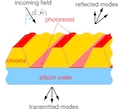
Applications in diffractive optics
Diffractive optical elements employ the controlled use of light propagation on microstructered interfaces and can be applied in diffractive measurement technique, spectroscopy, astronomy, optical communication techniques, etc. These elements are manufactured with photolitography method, relying, in turn on precise knowledge of the optic properties of the materials. Our joint effort with the cooperation partners from PTB is in mathematical modelling and numeric simulations of the measurement process. A statistical description of the measurement result can be given as a solution of a Bayesian inverse problem. We focus on developing and applying novel methods of Bayesian inversion, stemming from optimal transport ang gradient flow theory.
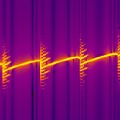
Dynamics of semiconductor lasers
Semiconductor lasers are compact, efficient and reliable light sources playing a crucial role in many modern technological systems. Depending on parameters and on their geometry, laser devices demonstrate a variety of complex dynamical regimes. A comprehensive study of the underlying nonlinear processes and bifurcation analysis leads to a better understanding of the observed behavior. This knowledge supports the design of new types of laser devices for specific purposes.
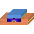
Modeling and simulation of semiconductor structures
Modern semiconductor and optoelectronic devices such as semiconductor lasers or organic field-effect transistors are based on semiconductor structures, which e.g. can be given by doping profiles, heterostructures or nanostructures. For the qualitative and quantitative understanding of the properties of these devices, mathematical modeling and simulation of the most relevant and, respectively, of the limiting carrier transport processes is necessary. In the context of the Green Photonics Initiative new topics move into the focus of research, e.g. reduced energy consumption of devices, new applications in the field of renewable energies, communication and lighting.
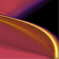
Optical pulses in nonlinear media
This application deals with extreme nonlinear optics, and in particular with the propagation of intense ultrashort pulses in optical fibers. The propagation and stability of these pulses are studied by novel numerically effective models, which correctly account for both nonlocal response effects and basic physical constraints. For the latter, it is important to keep the causality principle, leading to the intrinsic Kramers-Kronig relation between dispersion and dissipation. In addition, the correct behavior of the medium response for large frequencies should be reproduced by the model. Furthermore, propagation equations are used to investigate long-living solitary solutions and mutual interactions of extreme few-cycle optical pulses.
Quantum models for semiconductors
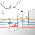
Mathematical modeling of electrons in semiconductor nanostructures and molecules requires a quantum mechanical description using the Schrödinger equation. In semiconductors, e.g., the electronic band structure, which determines the functionality of devices, can be understood by this means. The simulation of time-dependent processes such as the coherent evolution of electrons in semiconductor nanostructures or the evolution of chemical reactions is of major interest in numerous applications. Modeling dissipative processes requires evolution equations for density matrices that describe the interaction of qauntum particles with their macroscopic environment.
Electronic materials
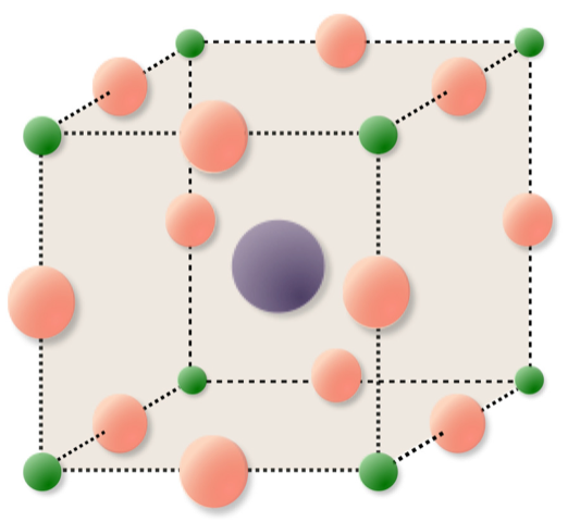
Novel electronic materials require advanced charge transport modeling and simulation techniques in which moving ions on the crystal lattice cannot be neglected. Examples of such materials are perovskites and 2D layered transition metal dichalcogenides (TMDCs) like molybdenum disulfide. They play a fundamental role for applications like solar cells as well as memristive devices.


