from left to right: Patricio Farrell, Dilara Abdel, Zeina Amer, Yiannis Hadjimichael, Imke Weitkamp
Overview
The Leibniz group NUMSEMIC develops and numerically solves nonlinear PDE models.
These models are often inspired by charge transport in innovative semiconductor devices.
In particular, applications include perovskite solar cells, memristors, nanowires,
quantum wells, lasers as well as doping reconstruction. To translate these applications into mathematical models,
we rely on nonlinear drift-diffusion, hyperelastic material models, inverse PDE problems, localized landscape theory
and atomistic coupling.
Our methodologies include physics-preserving finite volume methods, data-driven techniques as well as meshfree
methods.
Mathematical research topics
Modeling with and numerical solution of nonlinear systems of partial differential equations
Nonlinear drift-diffusion models, hyperelastic materials, inverse PDE problems, localized landscape theory and
atomistic coupling
Physics preserving finite volume methods on Voronoi meshes
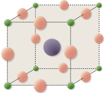
Charge transport in semiconductors
Preconditioners and anisotropic meshing strategies
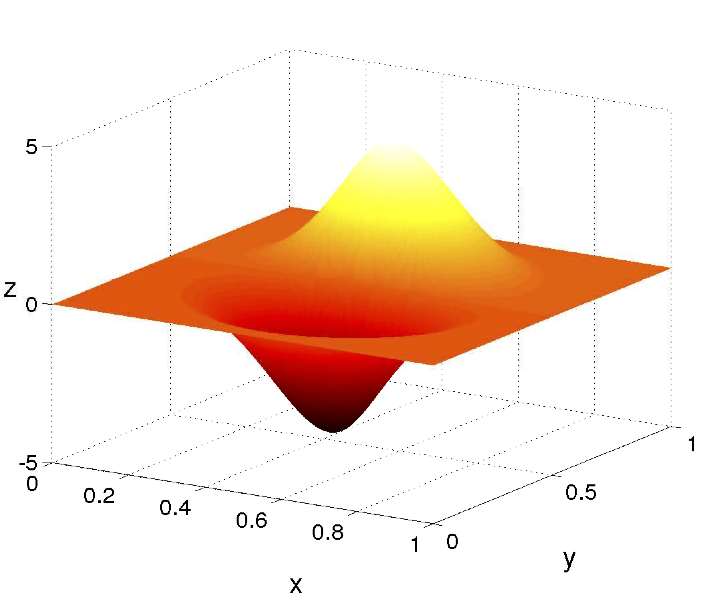
High dimensional meshfree approximation
Data-driven techniques for ill-posed inverse problems
Applications
Perovskites: About ten years ago engineers showed for the first time that low-cost perovskites could be used
to convert
sunlight into electricity. Since then their efficiency has greatly improved, giving hope to replace or modify (via
tandem solar cells) less efficient yet widely-used silicon-based solar cells soon. Simulating perovskite solar cells
is extremely challenging due to stiffness: Apart from electrons and holes a third ionic species has to be considered
which moves about twelve orders of magnitude more slowly. This means that different time scales are present in the
model which leads to numerical difficulties.
Cooperations: RG1, RG3, Helmholtz Zentrum Berlin, Zuse Institute Berlin, University of Oxford, Inria Lille/University of Lille
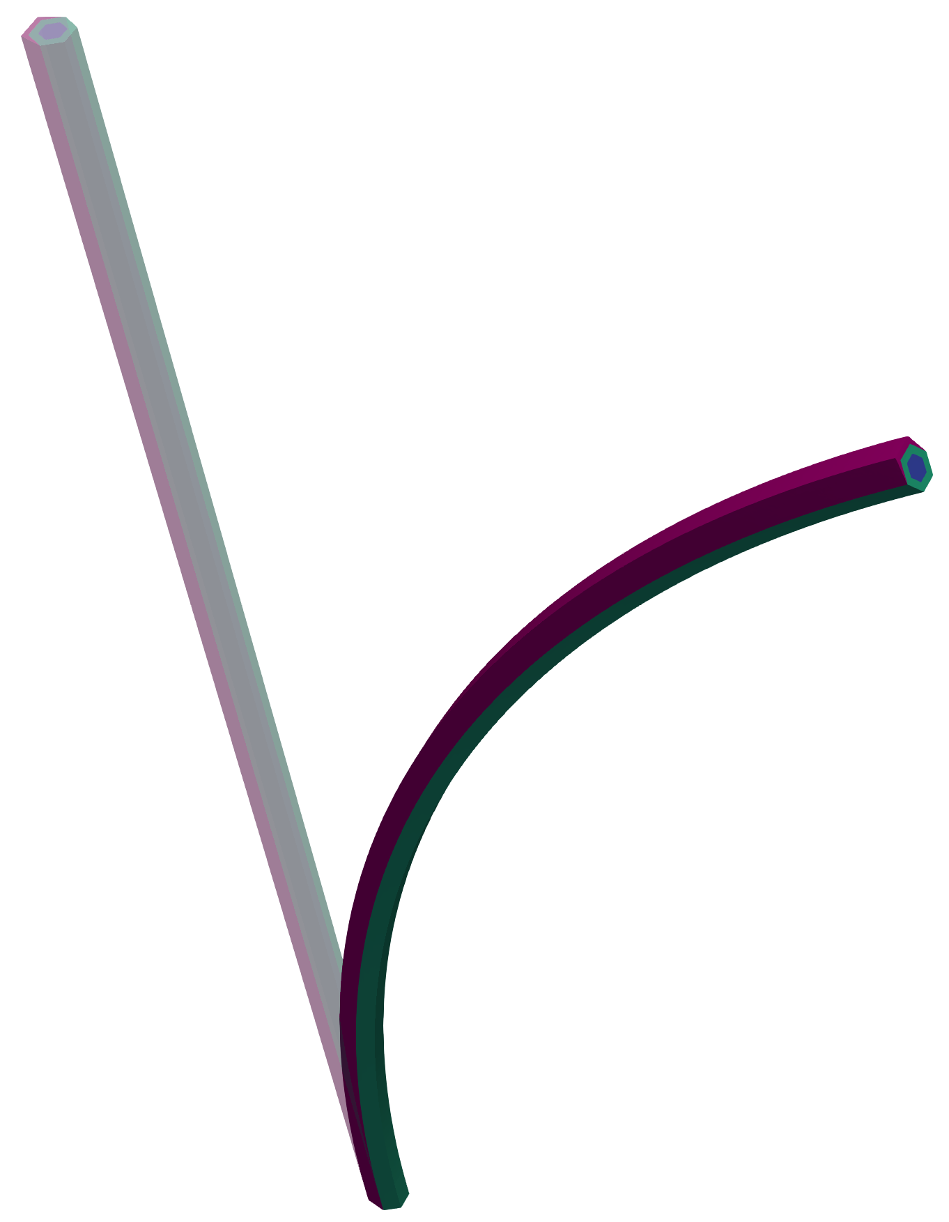
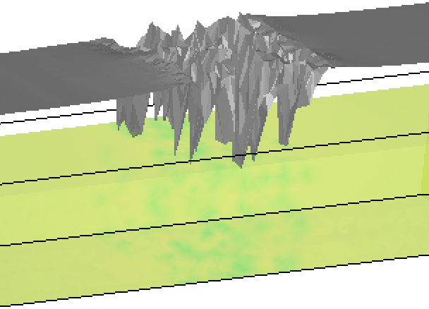
Nanowires: Nanowires have many potential applications, for example they may be used to build even smaller MOS
transistors. Useful electronic properties of these thin wires can be controlled via elastic strain. For example,
bending nanowires changes the band gap. However, deformation-related, piezoelectric, and in particular flexoelectric
contributions create a complicated potential landscape which is poorly understood and leads to unexpectedly slow
charge carrier transport. Careful simulations combining charge transport with continuum mechanics are needed to
explain the cause.
Cooperations: RG1, RG3, Paul-Drude-Institut
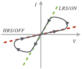
Memristors: The von Neumann architecture is far from ideal for AI applications due to its unacceptably high
energy consumption. Memristors help to emulate the extremely
efficient computing power of human brains. We develop complex charge
transport models which incorporate mobile point defects and Schottky barrier lowering to theoretically understand
the shape and asymmetries of the hysteresis curves observed in experiments.
Cooperations: TU Ilmenau
Quantum wells: We model and simulate random alloy fluctuations in band edge profiles within a full device. To
achieve this, we combine random atomic fluctuations in band edges with macroscale drift diffusion processes. The
spatially randomly varying band edges are implemented in ddfermi. Quantum effects are taken into account via
localization landscape theory (LLT).
Cooperations: RG1, Tyndall National Institute (Cork, Ireland)
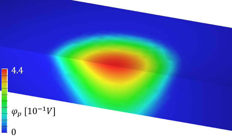
Imaging techniques: We model several semiconductor-based imaging techniques to predict fluctuations in doping
profiles such as the laser beam induced current (LBIC) or the lateral photovoltage scanning (LPS) method.
Mathematically, we need to solve an inverse problem which we achieve via machine learning techniques.
Cooperations: RG3, Institut für Kristallzüchtung, University of Florence, SISSA (Trieste, Italy)
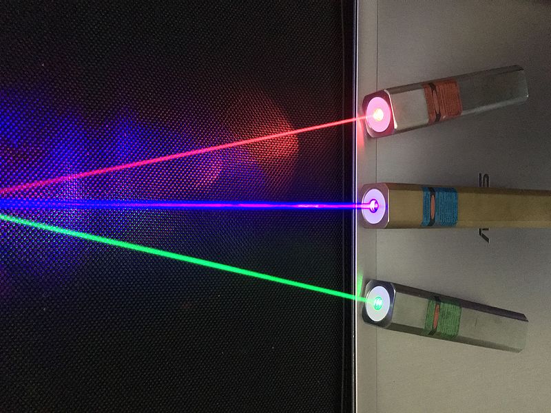
Source: Pang Kakit (CC BY-SA 3.0)
Lasers: Semiconductor lasers are needed in many areas: For example,
semiconductor-based LiDAR (light detection and ranging) sensors improve autonomous driving as they are accurate,
comparatively small and thus mass market friendly. Moreover, high precision lasers are needed in quantum metrology
and quantum computing. Our group extends the van Roosbroeck model to incorporate additional physical effects
(heterostructures, heat transport and light emission). In particular, we couple our charge transport model with a
Helmholtz problem.
Cooperations: RG1, RG2, RG3, Ferdinand-Braun-Institut
Neural networks/surrogate models: The core of machine learning algorithms consists of a (usually
high-dimensional) optimization problem. To find a
minimizer within such complex structures it is often beneficial to resort to surrogate models, which will be
minimized
instead of the original problem. Due to the curse of dimensionality it is often not feasible to build meshes. For
this
reason meshfree methods help to efficiently build surrogate models for high-dimensional problems. Additionally, we
solve inverse problems arising semiconductor-based imaging techniques via machine learning techniques.
Cooperations: WG DOC, University of Florence, SISSA
In December 2025, Patricio Farrell represented the German node at the EU-MATHS-IN Council Meeting in Cyprus to strengthen industrial mathematics within the European Union via strategic policies.
September 2025: Patricio Farrell co-organizes the QuaSy2025 workshop in Florence. Dilara Abdel and Zeina Amer are invited as speakers.
In June 2025, Dilara Abdel was an invited speaker in first mini workshop within the ARISE Associate Team". She visited RAPSODI Inria for two weeks
In April 2025, a paper by Dilara Abdel and Patricio Farrell, in collaboration with researchers from TU Ilmenau, was ranked among the top 10% most-viewed publications in 2023 by Advanced Electronic Materials.
In April 2025, Dilara Abdel and Patricio Farrell participated in the AMPD2025 Workshop.
In March 2025, Kees Vuik from Delft University of Technology visited the NUMSEMIC group.
In November 2024, Patricio Farrell was elected vice chair of the Committee for Mathematical Modeling, Simulation and Optimization (KoMSO)
In September 2024, Albert Pool from German Aerospace Center (DLR) visited the NUMSEMIC group.
In September 2024, the AMaSiS conference took place, organized by WIAS.
In July 2024, Julien Moatti from TU Vienna visited the group for a week.
Zeina Amer and Yiannis Hadjimichael presented at the MMS Days.
Dilara Abdel successfully defended her PhD at Freie Universität Berlin. The title of her thesis is Modeling and simulation of vacancy-assisted charge transport in
innovative semiconductor devices.
In September 2022, Dilara Abdel and Yiannis Hadjimichael presented talks at the online conference NUSOD 2022 conference. An additional submission together with Julien
Moatti, Inria Lille, was voted among the top 10 contributions.
In summer 2022, Julien Moatti from Inria Lille visited
the group for three months.
In spring 2022, Stefano Piani from SISSA visited the
group twice.
In June 2022, Yiannis Hadjimichael was invited to present a talk the SDIDE 2022
workshop.
The Leibniz group is organizing a mini symposium at the SIAM Conference on Mathematical Aspects of Materials
Science 2021 with the title Modelling and simulation of charge transport in perovskites. Dilara Abdel
won a SIAM MS student travel award for attending the conference to give a talk.