WIAS Research Highlights
Numerical Methods for Innovative Semiconductor Devices - An Outlook
Introduction
Few discoveries have shaped our modern society like semiconductors. They are the backbone of every electronic device. A world without semiconductors would be one without television, pacemakers, satellites, solar cells, cell phones, air planes, computers - and, by extension, a world without the Internet, social media, and online communication. Semiconductors have made come true what our ancestors would have considered magic. The numbers corroborate this: The global semiconductor industry is huge - world-wide sales topped $400 billion in 2017 for the first time.
Semiconductors are electronic materials that can act as either conductors (like copper) or insulators (like glass). The conductivity may be controlled, for example, by temperature, intentionally introduced impurities (the doping) or even sunlight. This special feature of sometimes resembling metal and sometimes insulators is exploited by practically all electronic components. For this reason it is fundamentally important to model, analyze, and simulate semiconductors correctly. In the past decades, many researchers have worked on models, their analysis and simulations.
How charge carriers (electrons and holes) flow in a semiconductor is modeled by the basic semiconductor equations, also known as the van Roosbroeck system [1]. It consists of three nonlinearly coupled partial differential equations (PDEs): one self-consistent equation for the electrostatic potential and two continuity equations for electrons and holes, respectively. The model incorporates two types of movements. Charge carriers drift because the electric field pushes them and diffuse from areas of high to areas of low concentrations.
Since usually no analytic solution is known, one has to solve the continuous PDE system numerically. Any numerical solution shall preserve as many physical properties from the continuous van Roosbroeck system as possible. The finite volume method accomplishes this task in many ways. However, to avoid instabilities (the inevitable impact of rounding errors), a correct approximation of the charge carrier fluxes within the finite volume framework is crucial. The Scharfetter-Gummel flux scheme [2] is well-established for linear diffusion.
Unfortunately, in practice, linear diffusion is often a severe oversimplification. In physically challenging situations, such as very low temperatures, highly doped areas, or organic semiconductors (e.g., organic light-emitting diodes (OLEDs)), the diffusion becomes nonlinear, meaning that electrons and holes diffuse several orders faster when highly concentrated. Due to this diffusion enhancement, it is no longer possible to use the simplifying Boltzmann approximation. Instead, one has to resort to the more complicated Fermi-Dirac statistics. Finding physically correct (in particular, thermodynamically consistent) flux approximations for nonlinear diffusion is of extreme importance to avoid unphysical behavior. Yet several flux approximations proposed in the literature do not consider nonlinear diffusion. Recently, we constructed several such flux approximations and analyzed how they perform [3, 4, 5, 6]. These methods are needed in several cutting-edge applications, which drive the development of new numerical techniques and computational tools.
Accurate models and physically precise numerical techniques for semiconductor applications - such as the ones described in the preceding paragraph - were the very starting point for the new Leibniz Group LG 5 Numerical Methods for Innovative Semiconductor Devices, which was successful within the Leibniz competition. In this article, we give an overview of the group's different thematic key aspects, namely
- innovative applications,
- physical and computational challenges,
- and methodologies.
Applications
Innovative materials, devices and designs. Several promising technological and electronic innovations require to extend the PDE models presented in the introduction:
- About ten years ago, engineers showed for the first time that low-cost perovskites could be used
to convert sunlight into electricity. Since then, their efficiency has greatly improved, giving hope
to replace or modify (via tandem solar cells) less efficient yet widely used silicon-based solar
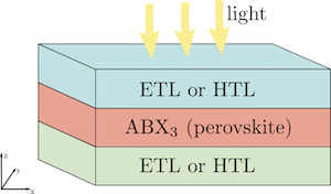
cells soon; see Figure 1 for a simplified perovskite-based solar cell (PSC). Perovskites are not
only a novel alternative to silicon in solar cells, but have alsomany additional useful properties.
They can store energy (leading to photo batteries, which may generate and store electric charge
generated by solar energy), act as magnets or lasers, and are investigated for data storage.
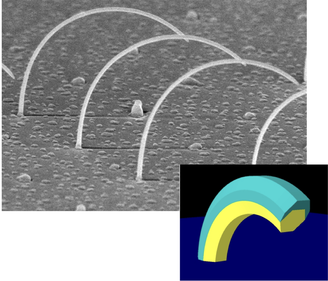
Simulating perovskite solar cells is extremely challenging due to stiffness. Apart from electrons and holes, a third ionic species has to be considered that moves about twelve orders of magnitude more slowly. This means that different time scales are present in the model, which leads to numerical difficulties. While initial attempts have been undertaken to simulate perovskite solar cells, the group plans together with researchers from Imperial College London to combine existing ideas with a Scharfetter-Gummel-type finite volume discretization as well as Fermi-Dirac statistics to account for nonlinear diffusion. Our partners at Helmholtz-Zentrum Berlin will enrich our simulations with experimental data and relevant research questions from applications. - Nanowires have the potential to greatly reduce the amount of bulk silicon needed in established solar cells, thus enabling cheaper and more resource-efficient solar cells. Useful electronic properties of these thin wires can be controlled via elastic strain. For example, bending nanowires changes the band gap. The Paul Drude Institute for Solid State Electronics (PDI) studies novel techniques to produce bent nanowires. However, deformation-related, piezoelectric, and, in particular, flexoelectric contributions create a complicated potential landscape, which is poorly understood and leads to unexpectedly slow charge carrier transport. In experiments, electrons and holes drift about three orders of magnitude slower than expected. Careful simulations are needed to explain the cause. In addition to charge transport (via the van Roosbroeck system), the strain of the material must also be modeled. Since experiments are often conducted at very low (cryogenic) temperatures, our techniques for nonlinear diffusion are indispensable.
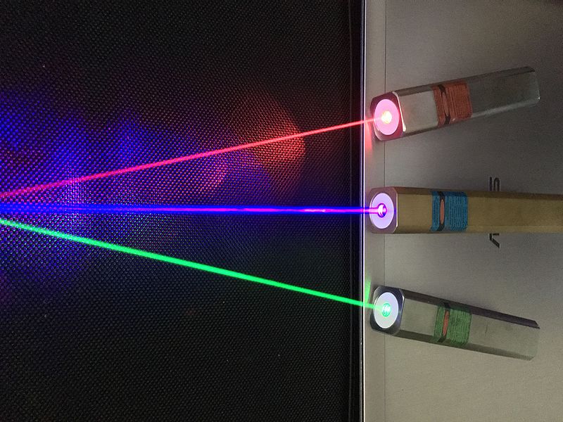
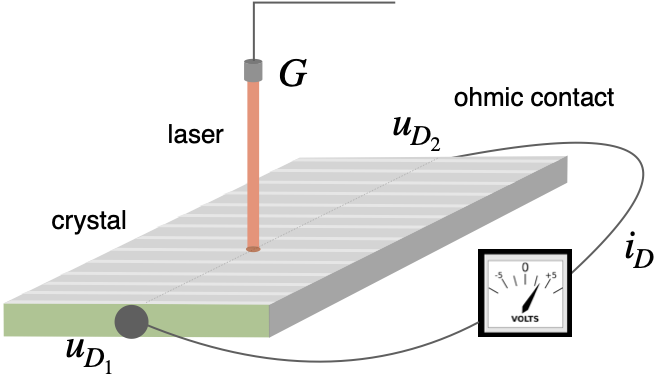
- Semiconductor lasers are needed in many areas: For example, our collaborators at the Ferdinand-Braun-Institut für Höchstfrequenztechnik study semiconductor-based LiDAR (light detection and ranging) sensors that are expected to improve autonomous driving, since they are accurate, comparatively small, and thus mass-market friendly. Moreover, high precision lasers are needed in quantum metrology and quantum computing. Since building new laser prototypes is costly, it is important to understand for all these cases how a new setup works before production. Thus, simulations of semiconductor lasers will not only provide scientific insights, but also help to reduce development costs. To this end, the group will extend the van Roosbroeck model to incorporate more than two charge-carrier species and include additional physical effects (heterostructures, heat transport, and light emission). New physics-preserving numerical methods will be developed to account for these extensions. For efficiency different physical effects need to be resolved on different scales. Fig. 4: The lateral photovoltage scanner
- The lateral photovoltage scanning (LPS) method helps to reconstruct tiny fluctuations within a semiconductor crystal such as silicon. This knowledge is important because it provides insight into how the temperature field is distributed during the growth of a semiconductor crystal. Given that silicon melts at 1687K, it is impossible to measure the temperature directly. Therefore, the crystal growth community tries to infer the temperature distribution post mortem from these fluctuations, so-called striations, within the crystal. The idea is that within an inhomogeneous material a laser hitting the surface of a crystal sample will generate a voltage that can be measured. After scanning the sample at various laser spot positions, one may use the data to predict the distribution of the fluctuations without having to slice and thus destroy the expensive crystal. The LPS setup is shown in Figure 4.
Mathematical, physical and computational challenges
In summary, these innovative applications call for several extensions of the van Roosbroeck system on many different levels that the group will be focusing on:
- Diverse additional physical effects (such as heat transport, elastic strain, and light emission) will be modeled consistently, investigated numerically and simulated efficiently.
- New types of charge carriers, such as heavy holes or ions, which may move at a considerably slower speed than electrons and holes, will be modeled and incorporated in a simulation tool (multispecies aspect).
- Different spatial resolutions for different physical effects (multiscale aspect) as well as layers of various types of materials will be considered (heterostructures).
- We allow that some parameters in the original PDE model, e.g., the doping, are not known a priori, changing the character of the original model entirely (inverse problem).
Methodologies
Physics preserving numerical methods. For a given application, the corresponding models need to be converted into a language that computers can interpret. This process is called discretization, which turns a continuous problem into a discrete one. The discrete problems are associated with a discrete version of the domain (the mesh). Finite volume methods have the advantage that for vanishing source terms they preserve electron and hole fluxes discretely from one region to another - just as physics dictates. On the one hand, with a Voronoi mesh, they can be used efficiently. On the other hand, they lead to stable discretizations, which means that inevitable rounding errors do not easily corrupt the solution. This fact allows to develop new numerical methods that correctly preserve the physics - also when, in addition to nonlinear diffusion, other physical effects or additional charge carriers cannot be neglected.
Computational efficiency. Once the continuous models are discretized, it is imperative that a simulation program produces a solution as fast as possible. Carefully tailored preconditioning and meshing strategies help to achieve this task.
- Preconditioners help to reduce the computational cost by converting the discretized problem into a more suitable form for numerical computations. They are widely applied in numerical mathematics and indispensable for three-dimensional calculations, where it is no longer possible to employ direct solvers, since they scale highly unfavorably. Instead, one has to use iterative techniques, which adequate preconditioners speed up considerably. Unfortunately, preconditioners always have to be tailored to the specific numerical problem and cannot be used generically.
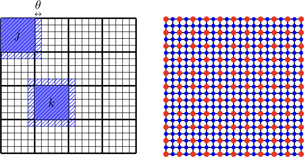
- To make the computations accurate and efficient, the mesh needs to be highly anisotropic, meaning that in areas where the solution varies strongly, we have to use more nodes to resolve the fluctuations. In areas where it varies slowly, we may use fewer nodes to reduce the size of the problem and thus the computational cost. This is especially important for boundary layers and multiscale effects. The aim is to let the computer as far as possible automatically decide where to refine the mesh and where to coarsen it. Despite its practical importance, automatic anisotropic mesh generation is still an open problem.
User-friendly, fast, and open-source simulations. When designing code, one often experiences the conundrum to write fast-running as well as user-friendly code. While established low-level languages like C/C++ are very fast, they are often not easy to use, require considerable experience, and the output is difficult to interpret. Other languages like MATLAB are intuitive and easy to learn, yet do not run very fast in comparison. MATLAB, in particular, is also proprietary software. Hence, an open-source simulation tool, which combines both advantages (fast run time and userfriendliness), is needed. Furthermore, the discrete systems are highly nonlinear. An established way to solve these systems is via Newton's method with parameter embedding. However, deriving the derivatives for the Jacobian takes time and is error-prone. Thus, ways to circumvent setting up the Jacobian are needed to save development time, lines of code, and possible sources of error. We will investigate new software solutions for automatic differentiation that programming languages such as Julia have to offer.
The future
The group has now until December 2024 to work out the details of the presented research program. First results can be found on page 113. It will collaborate with different research groups within WIAS that have already contributed significantly to the mathematics behind semiconductors such as RG 1 Partial Differential Equations, RG 2 Laser Dynamics, and RG 3 Numerical Mathematics and Scientific Computing. Apart from that, LG 5 will work together with Paul Drude Institute for Solid State Electronics, Ferdinand-Braun-Institut für Höchstfrequenztechnik, and Helmholtz-Zentrum Berlin für Materialien und Energie as well as with international partners from the University of Milano-Bicocca, Imperial College, and the University of Strathclyde. Future scientific interests include biosensors and physics-informed data-driven methods.
References
[1] W. VAN ROOSBROECK, Theory of the flow of electrons and holes in germanium and other semiconductors, Bell System Tech. J., 29:4 (1950), pp. 560-607.
[2] D. SCHARFETTER, H. GUMMEL, Large-signal analysis of a silicon read diode oscillator, IEEE Trans. Electron Devices, 16:1 (1969), pp. 64-77.
[3] P. FARRELL, T. KOPRUCKI, J. FUHRMANN, Computational and analytical comparison of flux discretizations for the semiconductor device equations beyond Boltzmann statistics, J. Comput. Phys., 346 (2017), pp. 497-513.
[4] P. FARRELL, D. PESCHKA, Nonlinear diffusion, boundary layers and nonsmoothness: Analysis of challenges in drift-diffusion semiconductor simulations, Comput. Math. Appl., 78 (2019), pp. 3731-3747.
[5] M. PATRIARCA, P. FARRELL, J. FUHRMANN, T. KOPRUCKI, Highly accurate quadrature-based Scharfetter-Gummel schemes for charge transport in degenerate semiconductors, Comput. Phys. Comm., 235 (2018), pp. 40-49.
[6] D. ABDEL, P. FARRELL, J. FUHRMANN, Assessing the quality of the excess chemical potential flux scheme for degenerate semiconductor device simulation, Opt. Quantum Electron., 53 (2021), pp. 163/1-163/10, Open Access: https://link.springer.com/article/10.1007/s11082-021-02803-4.