Collaborator:
H. Gajewski
,
H. Stephan
Cooperation with: G. Wachutka, W. Kaindl (Technische Universität München)
Supported by: DFG: ``Physikalische Modellierung und numerische Simulation
von Strom- und Wärmetransport bei hoher Trägerinjektion und hohen
Temperaturen'' (Physical modeling and numerical simulation of current
and heat transport at high carrier injection and high temperatures)
[2]
Description:
In 2002 our model [1],
describing heat and carrier transport for semiconductor devices,
has been advanced to silicon carbide
(SiC). SiC is used in different crystal
configurations (6H-SiC, 4H-SiC, 3C-SiC). Each of these materials
possesses promising properties as basic materials for
high-power, high-temperature and high-frequency electronics.
The reason for this are special physical characteristics, which
distinguish SiC from conventional semiconductor materials such as silicon.
Those are first of all:
- Anisotropy:
For each crystal configuration it is typical that physical
quantities, such as carrier mobilities or heat conductivity,
depend on the crystal orientation. It follows that
appropriate physical quantities are no longer scalars but
tensors. For example, the electron mobility in the hexagonal plain of
4H-SiC is five times larger than in the perpendicular direction.
- Wide band gap:
The band gap in SiC is up to 3.2 eV (for comparison, the band gaps in
Si and GaAS are 1.1 eV and 1.42 eV, respectively). This makes the material
interesting for optoelectronics
(blue LEDs). However,
numerical problems can arise, since the gap enters exponentially
into the equations of state. Additionally, the wide gap
may lead to an only incomplete ionization of the dopants (in
particular boron).
This means, dopants have to be considered as traps.
- High temperature resistance: This--very welcome
characteristic--requires the consideration of a large parameter area
for temperature dependence of material data for the simulation.
Deriving the system of nonlinear partial differential equations
for the heat and carrier transport in semiconductor devices,
we abided by the following physical principles:
- 1.
- postulation of the free energy density;
- 2.
- calculation of the equilibrium according to
the entropy maximum principle;
- 3.
- definition of the thermodynamic potentials near the equilibrium state;
- 4.
- postulation of the evolution equations;
- 5.
- calculation of the currents and right-hand sides
according to the second law of thermodynamics;
- 6.
- derivation of the heat equation.
The postulated system of equations
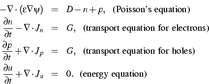
describes electron, hole and
energy transfer, which is nonlinearly coupled by the
electrostatic potential  via Poisson's equation. Here,
n, p and u are electron, hole and power density,
Jn, Jp and Ju the appropriate currents, D the dopants
and G the generation-recombination rate. (The ODEs describing
the dynamics of electron/hole traps were described
in detail in the WIAS Annual Research Report 1998.)
via Poisson's equation. Here,
n, p and u are electron, hole and power density,
Jn, Jp and Ju the appropriate currents, D the dopants
and G the generation-recombination rate. (The ODEs describing
the dynamics of electron/hole traps were described
in detail in the WIAS Annual Research Report 1998.)
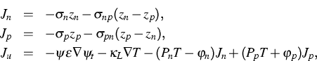
The determination of the equilibrium as state of maximal entropy
by Lagrange's method suggests the Lagrange multipliers
 ,
,  and
and  to be thermodynamic potentials. Their gradients are the driving
forces for the currents. That leads to the following
current, under consideration of Onsager's principle:
to be thermodynamic potentials. Their gradients are the driving
forces for the currents. That leads to the following
current, under consideration of Onsager's principle:
![\begin{eqnarray*}
\left(
\begin{array}
{c}
\!\!J_n\!\! \ [1.2em]
\!\!J_p\!\! \...
...\!\displaystyle{-\nabla \frac{1}{T}}\!\!\ \end{array}\right)\; .\end{eqnarray*}](img58.gif)
In the case of the anisotropic SiC,
 ,
, and
and  , and
anu, anp and au are
, and
anu, anp and au are  matrices.
From the second law of thermodynamics
(entropy S increasing in time)
matrices.
From the second law of thermodynamics
(entropy S increasing in time)
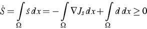
(here d denotes the dissipation rate) it follows for the currents
with

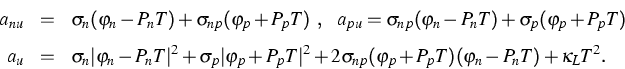
and the energy carrier interaction terms
( is the heat conductivity)
For this model, thermodynamically consistent algorithms were developed
and implemented into our program system
WIAS-TeSCA .
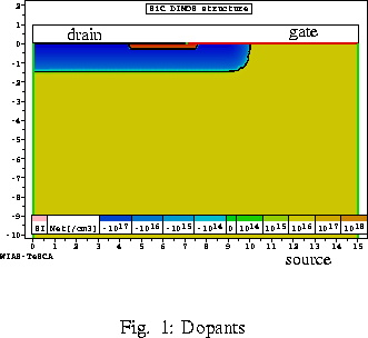
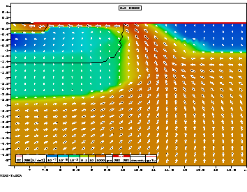
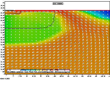
As an example we show a 6H-SiC DIMOS transistor--a
typical high-power device ([4]). The
crystal is oriented in such a way that the electron
mobility in horizontal direction is five times higher than in the
vertical direction. Figure 2 shows the electron flow for a gate
voltage of 12 V and a drain voltage of 30 V. In comparison, Figure 3
shows the simulation result for isotropic mobility (e.g., in Si).
Fig. 2:
Anisotropic case
|
|
Fig. 3:
Isotropic case
|
|
References:
- G. ALBINUS, H. GAJEWSKI, R. HÜNLICH,
Thermodynamic design of energy models of semiconductor devices,
Nonlinearity, 16 (2002), pp. 367-383.
- H. GAJEWSKI, G. WACHUTKA,
DFG-Antrag zum Projekt ``Physikalische Modellierung und numerische
Simulation von Strom- und Wärmetransport bei hoher Trägerinjektion
und hohen Temperaturen'', 1996, 1998, 2000 (applications for a DFG project).
- H. GAJEWSKI, Analysis und Numerik des
Ladungsträgertransports in Halbleitern, GAMM-Mitteilungen, 16
(1993), pp. 35-57.
- M. LADES, Modelling and simulation of wide
bandgap semiconductor devices: 4H/6H-SiC, Shaker Verlag, Aachen 2002.
- G. WACHUTKA,
Rigorous thermodynamic treatment of heat generation and conduction in
semiconductor device modeling, IEEE Trans. on CAD, CAD-9 (1990),
pp. 1141-1149.
LaTeX typesetting by I. Bremer
5/16/2003