|
|
|
[Contents] | [Index] |
Cooperation with: F. Fidorra, Ch. Radüge (MergeOptics GmbH, Berlin), J. Kreissl (Heinrich-Hertz-Institut für Nachrichtentechnik (HHI) Berlin GmbH)
Supported by: MergeOptics GmbH
Description:
Investigations on InP-based 1.55 ![]() -emitting Ridge Waveguide
semiconductor lasers
with strained Multi Quantum Well active region by MergeOptics GmbH have
been performed for improving their performance.
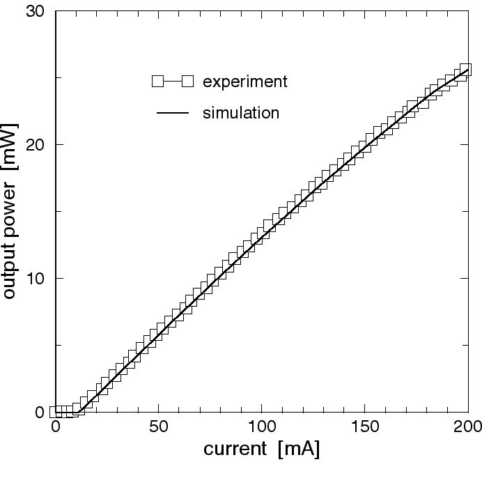
The simulations have been based on the device simulator
WIAS-TeSCA,
which allows for a selfconsistent treatment of the optical, electrical,
and thermal behavior of
semiconductor devices (see Fig.1).
-emitting Ridge Waveguide
semiconductor lasers
with strained Multi Quantum Well active region by MergeOptics GmbH have
been performed for improving their performance.
The simulations have been based on the device simulator
WIAS-TeSCA,
which allows for a selfconsistent treatment of the optical, electrical,
and thermal behavior of
semiconductor devices (see Fig.1).
![\makeatletter
\@ZweiProjektbilderNocap[h]{0.48\linewidth}{fb01_02_merge_jp.eps.gz}{fb01_02_merge_T_distri.eps.gz}
\makeatother](../2001/img3.gif)
|
Based on this fact, further simulations have been used to predict properties
with relevance for applications of possible future devices with changed
geometry.
|
Using the optical field distribution at the facet of the laser, which has been obtained as one of the outputs of WIAS-TeSCA, also the farfield distribution has been calculated in a postprocessing procedure ([1]). Again, such farfield distributions have been compared with experimental data which have been obtained from measurements at HHI. Some typical farfield intensity patterns are displayed within Fig.3.
Basic farfield characteristics, as
FWHM![]() -parameters
and
basic diffraction effects could be reproduced by the simulations
in good agreement with the measurements, see Fig.3.
However, some details, especially of the vertical
farfield intensity pattern (Fig.3, right)
are very difficult to be resolved by the model implemented so far.
For the investigation of such effects future work would be required.
-parameters
and
basic diffraction effects could be reproduced by the simulations
in good agreement with the measurements, see Fig.3.
However, some details, especially of the vertical
farfield intensity pattern (Fig.3, right)
are very difficult to be resolved by the model implemented so far.
For the investigation of such effects future work would be required.
References:
|
|
|
[Contents] | [Index] |
![\makeatletter
\@ZweiProjektbilderNocap[h]{0.48\linewidth}{fb01_02_merge_ff00.eps}{fb01_02_merge_ff90.eps}
\makeatother](../2001/img5.gif)