|
|
|
[Contents] | [Index] |
Collaborator: U. Bandelow (FG 1), M. Baro (FG 1), Th. Koprucki (FG 3)
Cooperation with: J. Tomm and F. Weik (both Max-Born-Institut für Nichtlineare Optik und Kurzzeitspektroskopie (MBI), Berlin), M. Grau (Walter-Schottky-Institut, Technische Universität München)
Supported by: MBI, DFG: Research Center MATHEON, project D4; Priority Program ``Analysis, Modellbildung und Simulation von Mehrskalenproblemen'' (Analysis, Modeling and Simulation of Multiscale Problems)
Description:
Indium-arsenide-antimonide (InAsSb) heterostructures, having the lowest band gap of all III-V semiconductors, are of great interest in the recent development of infrared optoelectronic devices like lasers and photodetectors. The aim of the project is the calculation of the electronic band structure of InAsSb multi-quantum-well (MQW) lasers.
The MQW structures we investigate are grown at the Walter Schottky Institute and are potential candidates for the optically active region of infrared LEDs. The structures consist of a stack of 10 -nm-thick strained InAsxSb1-x quantum wells sandwiched between 20 nm or 40 nm Al0.15In0.85As0.78Sb0.22 barriers. The arsenic content of the well material varies between the samples, which leads to a different strain for each sample. The investigation of the influence of the strain on the bandgap is a central point of the investigations.
Characterization and measurements of the structures are carried out at the Max Born Institute (MBI).
The most economical description of the energy bands in semiconductors
is the multiband k . p method.
According to this method the
quantum-confined states
F![]() l(z;
l(z;![]() ) and the
corresponding subband dispersions
El(
) and the
corresponding subband dispersions
El(![]() ) are solutions of
the respective eigenvalue problem
) are solutions of
the respective eigenvalue problem
![\minipage{0.6\textwidth}%
\ZweiProjektbilder [v]{.9\linewidth}{A0650-cb}{A0650-...
...ifferent directions
of ${\bf k_\Vert}$ of our selected sample}%
\endminipage](img740.gif) Our simulation parameters are obtained from Vurgaftman et al. [4]
by means of the ternary and quaternary interpolation schemes described there.
The bandgap Eg and the spin-split-off energy are obtained by
quadratic interpolation, whereas the remaining material parameters are
derived by linear interpolation.
For the calculations, the in-plane strain
is determined by the formula (a0 - a)/a, where
a0 = 0.6096 nm
is the lattice constant of the GaSb substrate, and a is the lattice
constant of the corresponding layer material.
The calculated strain values agree with the measured values.
The calculated bandgap varies linearly with the strain, with a slope of
about
84 meV, which compares well with the experimental findings
obtained by MBI, [5].
Our simulation parameters are obtained from Vurgaftman et al. [4]
by means of the ternary and quaternary interpolation schemes described there.
The bandgap Eg and the spin-split-off energy are obtained by
quadratic interpolation, whereas the remaining material parameters are
derived by linear interpolation.
For the calculations, the in-plane strain
is determined by the formula (a0 - a)/a, where
a0 = 0.6096 nm
is the lattice constant of the GaSb substrate, and a is the lattice
constant of the corresponding layer material.
The calculated strain values agree with the measured values.
The calculated bandgap varies linearly with the strain, with a slope of
about
84 meV, which compares well with the experimental findings
obtained by MBI, [5].
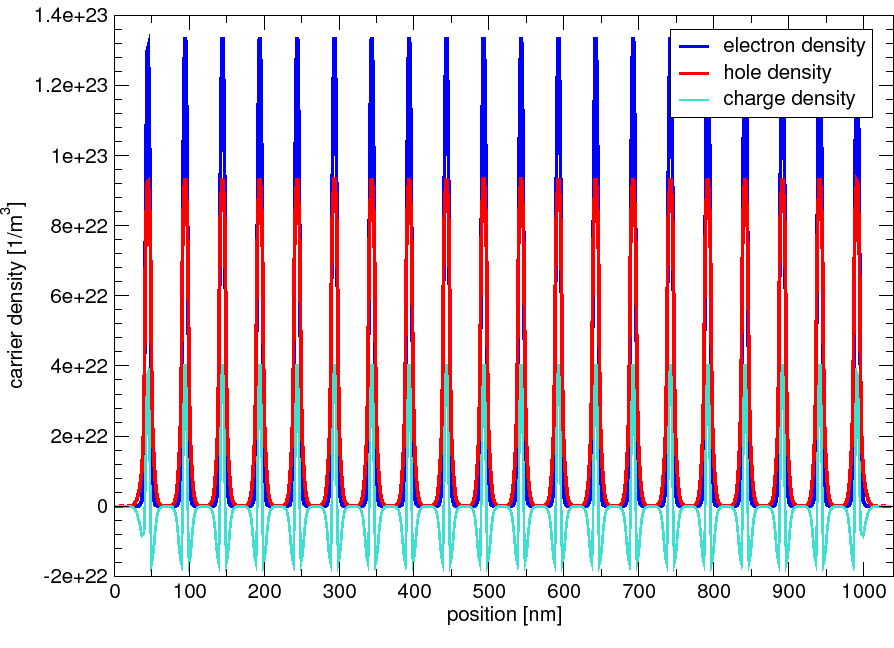
As an example, we plot the subband structure of one sample in Figure 1. It exhibits a strong nonparabolicity, especially for the valence subbands. For the latter, also strong warping (angular dependence) is detected, which is also a result of the band-band interaction, which involves electrons, heavy holes, light holes, and spin-split-off holes.
For further illustration, we plot the local density distributions within the
MQW structures for our selected sample in Figure 1.
For these illustrations, we assume charge neutrality
with sheet densities given by
N = P = 1011/cm2.
We observe very good confinement of the electrons as well as of the holes
within the quantum wells.
That is, their difference (which is the net charge density) remains
small and not much screening takes place.
As can also be seen by the density distribution in Figure 2,
the quantum wells are well isolated from each other by the barriers,
such that calculations with single quantum wells yield the same results as
calculations on the full MQW structure.
 |
References:
|
|
|
[Contents] | [Index] |